Hardware: Difference between revisions
Jump to navigation
Jump to search
mNo edit summary |
|||
| Line 17: | Line 17: | ||
|} | |} | ||
{{:EMMC_pinout}} | |||
https://www.sosav.fr/guides/consoles/nintendo/nintendo-salon/nintendo-switch/demontage-complet/ | https://www.sosav.fr/guides/consoles/nintendo/nintendo-salon/nintendo-switch/demontage-complet/ | ||
https://www.ifixit.com/Teardown/Nintendo+Switch+Teardown/78263 | https://www.ifixit.com/Teardown/Nintendo+Switch+Teardown/78263 | ||
Revision as of 05:52, 14 March 2017
Specifications
| Type | |
|---|---|
| SoC | NVidia ODNX02-A2 |
| Screen | 6.2-inch, multi-touch capacitive LCD screen |
| Storage | Samsung KLMBG2JENB-B041 32 GB eMMC or Toshiba THGBMHG8C2LBAIL 32 GB eMMC |
| Wifi/BT | Broadcom BCM4356XKUBG |
| PMIC | Maxim Integrated MAX77620AEWJ+T |
| Audio | Realtek ALC5639 |
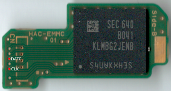
Front
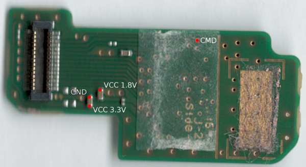
Back
Supply power via the VCC 3.3V and 1.8V pins, and solder the CLK, CMD, and DAT0 pins to an SD Card reader in order to extract the data off the eMMC chip.
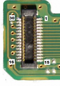
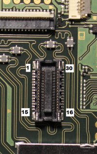
eMMC Connector


| Pin # | Name | Type |
|---|---|---|
| 1 | 3.3v | PWR |
| 2 | GND | PWR |
| 3 | CMD | BI |
| 4 | GND | PWR |
| 5 | DAT_STRB(?) | OUT |
| 6 | GND | PWR |
| 7 | DAT4 | BI |
| 8 | GND | PWR |
| 9 | DAT5 | BI |
| 10 | GND | PWR |
| 11 | DAT6 | BI |
| 12 | GND | PWR |
| 13 | DAT7 | BI |
| 14 | GND | PWR |
| 15 | 1.8v | PWR |
| 16 | 1.8v | PWR |
| 17 | GND | PWR |
| 18 | GND | PWR |
| 19 | DAT2 | BI |
| 20 | GND | PWR |
| 21 | DAT1 | BI |
| 22 | GND | PWR |
| 23 | DAT0 | BI |
| 24 | GND | PWR |
| 25 | DAT3 | BI |
| 26 | GND | PWR |
| 27 | CLK | IN |
| 28 | GND | PWR |
| 29 | RESET | IN |
| 30 | 3.3v | PWR |
The eMMC connector plug on the board mates with the receptacle on the Switch motherboard. The receptacle is a Molex 5009130302, and is available from retailers such as Digi-Key.
https://www.sosav.fr/guides/consoles/nintendo/nintendo-salon/nintendo-switch/demontage-complet/
https://www.ifixit.com/Teardown/Nintendo+Switch+Teardown/78263

