Gamecard: Difference between revisions
No edit summary |
|||
| (22 intermediate revisions by 7 users not shown) | |||
| Line 1: | Line 1: | ||
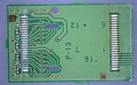
This page documents the Nintendo Switch Gamecard. | |||
{| style="float:right; margin-left: 0px;" | {| style="float:right; margin-left: 0px;" | ||
|- | |- | ||
| Line 77: | Line 10: | ||
|- | |- | ||
|[[File:CartridgeFrontBare.jpeg|200px|thumb|right|Close-up of stripped frontside PCB]] | |[[File:CartridgeFrontBare.jpeg|200px|thumb|right|Close-up of stripped frontside PCB]] | ||
|} | |} | ||
For the Gamecard image format, see [[XCI|here]]. | |||
For the Gamecard ASIC, see [[Lotus3|here]]. | |||
= Pinout = | |||
Note: Pins 1 and 2 act as one when receiving data from the ASIC chip. | |||
[[File:Gamecard-pinout.png|400px]] | [[File:Gamecard-pinout.png|400px]] | ||
| Line 90: | Line 27: | ||
! Description | ! Description | ||
|- | |- | ||
| | | 1 | ||
| | | GND | ||
| Input | |||
| Ground | |||
|- | |||
| 2 | |||
| CD# | |||
| Output | | Output | ||
| | | Card Detect; Single pin on cartridge side (hardwired to GND). Bridges pin 1 (GND) and 2 (CD#) on slot side as cartridge is inserted | ||
|- | |- | ||
| | | 3 | ||
| CLK | |||
| Input | |||
| Clock, 25MHz | |||
|- | |||
| 4 | |||
| RCLK | | RCLK | ||
| Output | | Output | ||
| Return clock; Game cartridge sends back CLK signal delayed by a few ns | | Return clock; Game cartridge sends back CLK signal delayed by a few ns | ||
|- | |- | ||
| | | 5 | ||
| | | CS# | ||
| Input | | Input | ||
| | | Chip Select | ||
|- | |- | ||
| | | 6 | ||
| | | DAT1 | ||
| | | Inout | ||
| | | Data bus pin 1 | ||
|- | |- | ||
| | | 7 | ||
| DAT0 | | DAT0 | ||
| Inout | | Inout | ||
| Data bus pin 0 | | Data bus pin 0 | ||
|- | |- | ||
| | | 8 | ||
| | | VCC 3.1v | ||
| Input | |||
| Power (3.1V) for Internal Core | |||
|- | |||
| 9 | |||
| DAT3 | |||
| Inout | | Inout | ||
| Data bus pin | | Data bus pin 3 | ||
|- | |||
| 10 | |||
| DAT2 | |||
|- | |||
| | |||
| DAT2 | |||
| Inout | | Inout | ||
| Data bus pin 2 | | Data bus pin 2 | ||
|- | |- | ||
| | | 11 | ||
| VCC 1.8v | |||
| VCC 1.8v | |||
| Input | | Input | ||
| | | Power (1.8V) for I/O | ||
|- | |- | ||
| | | 12 | ||
| DAT5 | | DAT5 | ||
| Inout | | Inout | ||
| Data bus pin 5 | | Data bus pin 5 | ||
|- | |||
| 13 | |||
| DAT4 | |||
| Inout | |||
| Data bus pin 4 | |||
|- | |- | ||
| | | 14 | ||
| DAT6 | | DAT6 | ||
| Inout | | Inout | ||
| Data bus pin 6 | | Data bus pin 6 | ||
|- | |- | ||
| | | 15 | ||
| DAT7 | | DAT7 | ||
| Inout | | Inout | ||
| Data bus pin 7 | | Data bus pin 7 | ||
|- | |- | ||
| | | 16 | ||
| GND | | GND | ||
| Input | | Input | ||
| Reset | | Ground | ||
|- | |- | ||
| 17 | |||
| RST# | |||
| Input | |||
| Reset | |||
|- | |||
|} | |} | ||
All IO use 1.8V for logic HIGH and 0V for logic LOW. | All IO use 1.8V for logic HIGH and 0V for logic LOW. | ||
== Protocol | Data pins are approximately 0.75mm in width and are in order of length: 9mm (pin 16), 8mm (pins 17, 5), 6mm (pins 1&2) 3mm (pins 3, 4, 6, 7, 9, 10, 12, 13, 14, 15). | ||
= Slot Pinout = | |||
[[File:Card_slot.jpg|500px|thumb|right|Annotated slot pinout]] | |||
This just maps the [[#Pinout|cartridge pinout]] onto the slot on the console. | |||
{| class="wikitable" | |||
! Pin | |||
! Name | |||
|- | |||
| 1 | |||
| GND | |||
|- | |||
| 2 | |||
| CD# | |||
|- | |||
| 3 | |||
| CLK | |||
|- | |||
| 4 | |||
| RCLK | |||
|- | |||
| 5 | |||
| CS# | |||
|- | |||
| 6 | |||
| DAT1 | |||
|- | |||
| 7 | |||
| DAT0 | |||
|- | |||
| 8 | |||
| VCC 3.1v | |||
|- | |||
| 9 | |||
| DAT3 | |||
|- | |||
| 10 | |||
| DAT2 | |||
|- | |||
| 11 | |||
| VCC 1.8v | |||
|- | |||
| 12 | |||
| DAT5 | |||
|- | |||
| 13 | |||
| DAT4 | |||
|- | |||
| 14 | |||
| DAT6 | |||
|- | |||
| 15 | |||
| DAT7 | |||
|- | |||
| 16 | |||
| GND | |||
|- | |||
| 17 | |||
| RST# | |||
|- | |||
|} | |||
= Protocol = | |||
Switch game cartridges use a simple (but Nintendo proprietery) SPI-like bus with 8-bit width (DAT7..0). It is very similar to the bus interface of 3DS game cartridges, except with very different commands. | Switch game cartridges use a simple (but Nintendo proprietery) SPI-like bus with 8-bit width (DAT7..0). It is very similar to the bus interface of 3DS game cartridges, except with very different commands. | ||
| Line 187: | Line 193: | ||
The actual response bytes are also followed immediately by a 4-byte CRC-32 over the actual data response bytes. | The actual response bytes are also followed immediately by a 4-byte CRC-32 over the actual data response bytes. | ||
= | = Manufacturers = | ||
;MegaChips (outsourced to Macronix) | |||
: Uses package: LGA, TSOP-48 | |||
: Uses card id: 0xC2 | |||
;Lapis | |||
: Uses package: LGA, TSOP-48 | |||
: Uses card id: 0xAE | |||
;LSI Logic (?) | |||
; | |||
: Uses package: LGA | : Uses package: LGA | ||
: Uses card id: | : Uses card id: 0x36 | ||
Latest revision as of 17:52, 21 August 2024
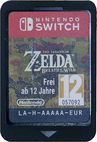
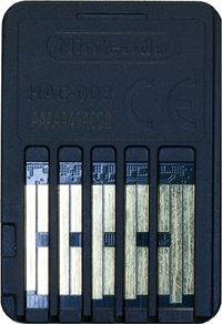
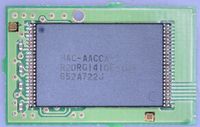
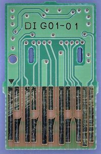
This page documents the Nintendo Switch Gamecard.
 |
 |
 |
 |
 |
For the Gamecard image format, see here.
For the Gamecard ASIC, see here.
Pinout
Note: Pins 1 and 2 act as one when receiving data from the ASIC chip.
| Pin | Name | Direction | Description |
|---|---|---|---|
| 1 | GND | Input | Ground |
| 2 | CD# | Output | Card Detect; Single pin on cartridge side (hardwired to GND). Bridges pin 1 (GND) and 2 (CD#) on slot side as cartridge is inserted |
| 3 | CLK | Input | Clock, 25MHz |
| 4 | RCLK | Output | Return clock; Game cartridge sends back CLK signal delayed by a few ns |
| 5 | CS# | Input | Chip Select |
| 6 | DAT1 | Inout | Data bus pin 1 |
| 7 | DAT0 | Inout | Data bus pin 0 |
| 8 | VCC 3.1v | Input | Power (3.1V) for Internal Core |
| 9 | DAT3 | Inout | Data bus pin 3 |
| 10 | DAT2 | Inout | Data bus pin 2 |
| 11 | VCC 1.8v | Input | Power (1.8V) for I/O |
| 12 | DAT5 | Inout | Data bus pin 5 |
| 13 | DAT4 | Inout | Data bus pin 4 |
| 14 | DAT6 | Inout | Data bus pin 6 |
| 15 | DAT7 | Inout | Data bus pin 7 |
| 16 | GND | Input | Ground |
| 17 | RST# | Input | Reset |
All IO use 1.8V for logic HIGH and 0V for logic LOW.
Data pins are approximately 0.75mm in width and are in order of length: 9mm (pin 16), 8mm (pins 17, 5), 6mm (pins 1&2) 3mm (pins 3, 4, 6, 7, 9, 10, 12, 13, 14, 15).
Slot Pinout
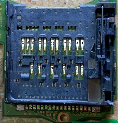
This just maps the cartridge pinout onto the slot on the console.
| Pin | Name |
|---|---|
| 1 | GND |
| 2 | CD# |
| 3 | CLK |
| 4 | RCLK |
| 5 | CS# |
| 6 | DAT1 |
| 7 | DAT0 |
| 8 | VCC 3.1v |
| 9 | DAT3 |
| 10 | DAT2 |
| 11 | VCC 1.8v |
| 12 | DAT5 |
| 13 | DAT4 |
| 14 | DAT6 |
| 15 | DAT7 |
| 16 | GND |
| 17 | RST# |
Protocol
Switch game cartridges use a simple (but Nintendo proprietery) SPI-like bus with 8-bit width (DAT7..0). It is very similar to the bus interface of 3DS game cartridges, except with very different commands.
The Switch host starts a transfer by first pulling CS low, followed by clocking a byte each clock cycle. The bus data will always be ready before the rising edge of the CLK signal, so that it can be captured on the rising edge. After command bytes are written to the bus, the direction of the bus implicitly changes and the game cartridge responds. The Switch host keeps clocking while the game cartridge responds. After the transfer is ended, the CS line is pulled high again.
Commands are 16 bytes long, and followed immediately by a 4-byte CRC-32 over the command bytes. After this, the Switch stops driving the data bus, and the bus will be 'floating'. Due to the pull-ups on the bus, it will slowly converge to logic HIGH state. The Switch will clock 2 cycles to allow the bus to settle a direction change. The Switch host will then clock another cycle and if the game cartridge didn't receive the CRC OK, it will respond with "01". Otherwise it will respond with "00" and pull DAT0 low on the next cycle to signal it is busy. The Switch host will then keep clocking until the cartridge is ready.
When the game cartridge is ready to send the actual data response, it will pull the DAT0 pin high for 2 cycles to let the Switch host know. After this, the game cartridge will send the actual data response bytes.
The actual response bytes are also followed immediately by a 4-byte CRC-32 over the actual data response bytes.
Manufacturers
- MegaChips (outsourced to Macronix)
- Uses package: LGA, TSOP-48
- Uses card id: 0xC2
- Lapis
- Uses package: LGA, TSOP-48
- Uses card id: 0xAE
- LSI Logic (?)
- Uses package: LGA
- Uses card id: 0x36
