Difference between revisions of "Gamecard"
(No difference)
|
Revision as of 22:14, 24 March 2018
For the Gamecard partitions that can be mounted, see here.
For the format of the Gamecard image, see here.
Firmware
FS is responsible for setting up the communication with the Gamecard. During this process, firmware blobs (with a fixed size of 0x7800 bytes) are loaded into some sort of programmable logic on the Gamecard.
The Gamecard firmware is encrypted, signed and follows the format below.
| Offset | Size | Description |
|---|---|---|
| 0x0 | 0x100 | RSA-PKCS#1 signature |
| 0x100 | 0x4 | Magic ("LAFW") |
| 0x104 | 0x4 | Unknown (0xFF000000, 0xFFFF0000 or 0xFFFFFF00) |
| 0x108 | 0x4 | |
| 0x10C | 0x4 | |
| 0x110 | 0x4 | Version (0, 1 or 3) |
| 0x114 | 0x4 | Unknown (0x80000000) |
| 0x118 | 0x4 | Data size |
| 0x11C | 0x4 | |
| 0x120 | 0x10 | Data hash |
| 0x130 | 0x10 | Unknown string ("IDIDIDIDIDIDIDID") |
| 0x140 | 0x40 | Empty |
| 0x180 | 0x7680 | Encrypted data |
Hardware
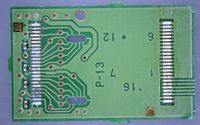
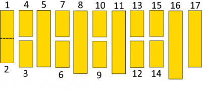
Pinout
| Pin | Name | Direction | Description |
|---|---|---|---|
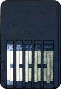
| 0 | IRQ? | Output | Always wired to GND inside game cartridge; Possibly used for interrupt signaling |
| 1 | RCLK | Output | Return clock; Game cartridge sends back CLK signal delayed by a few ns |
| 2 | CLK | Input | Clock, 25MHz |
| 3 | CS | Input | Chip select; Switch pulls this LOW during a transfer |
| 4 | DAT0 | Inout | Data bus pin 0 |
| 5 | DAT1 | Inout | Data bus pin 1 |
| 6 | VCC 3.3v | Input | |
| 7 | DAT2 | Inout | Data bus pin 2 |
| 8 | DAT3 | Inout | Data bus pin 3 |
| 9 | VCC 1.8v | Input | |
| 10 | DAT4 | Inout | Data bus pin 4 |
| 11 | DAT5 | Inout | Data bus pin 5 |
| 12 | DAT6 | Inout | Data bus pin 6 |
| 13 | DAT7 | Inout | Data bus pin 7 |
| 14 | GND | ||
| 15 | RST | Input | Reset, active LOW. |
All IO use 1.8V for logic HIGH and 0V for logic LOW.
Protocol
Switch game cartridges use a simple (but Nintendo proprietery) SPI-like bus with 8-bit width (DAT7..0). It is very similar to the bus interface of 3DS game cartridges, except with very different commands.
The Switch host starts a transfer by first pulling CS low, followed by clocking a byte each clock cycle. The bus data will always be ready before the rising edge of the CLK signal, so that it can be captured on the rising edge. After command bytes are written to the bus, the direction of the bus implicitly changes and the game cartridge responds. The Switch host keeps clocking while the game cartridge responds. After the transfer is ended, the CS line is pulled high again.
Commands are 16 bytes long, and followed immediately by a 4-byte CRC-32 over the command bytes. After this, the Switch stops driving the data bus, and the bus will be 'floating'. Due to the pull-ups on the bus, it will slowly converge to logic HIGH state. The Switch will clock 2 cycles to allow the bus to settle a direction change. The Switch host will then clock another cycle and if the game cartridge didn't receive the CRC OK, it will respond with "01". Otherwise it will respond with "00" and pull DAT0 low on the next cycle to signal it is busy. The Switch host will then keep clocking until the cartridge is ready.
When the game cartridge is ready to send the actual data response, it will pull the DAT0 pin high for 2 cycles to let the Switch host know. After this, the game cartridge will send the actual data response bytes.
The actual response bytes are also followed immediately by a 4-byte CRC-32 over the actual data response bytes.
Commands
A typical boot up sequence of a game cartridge (in this case, the game "1,2 Switch") looks like this:
| Command | Size | Description |
|---|---|---|
5B000000000000010000000000000000
|
0x200 | Read sector 0, contains "HEAD" blob |
5B000000000000010000000000000000
|
0x200 | Read sector 0, contains "HEAD" blob |
56000000000000000000000000000000
|
0x4 | Read card id "AE F8 01 21" |
28000000000000000000000000000000
|
0x4 | Read ??? "02 00 00 00" |
A5000000000000000000000000000000
|
0x4 | Read ??? "00 00 00 00" |
56000000000000000000000000000000
|
0x4 | Read card id "AE F8 01 21" |
28000000000000000000000000000000
|
0x4 | Read ??? "02 00 00 00" |
5B000000380000010000000000000000
|
0x200 | Read sector 0x38, contains "CERT" blob |
E2000000000000000000000000000000
|
0x4 | Read ??? "01 00 00 00" |
E0000000000000000000000000000000
|
0x200 | Read crypto-challenge header |
200838A25A344F818ABB6456694D4E8D
|
0 | Enter crypto mode1 with HOST-RANDOM "0838A25A344F818ABB6456694D4E8D" |
7EE41FDF12C01C157CC899910673A0CF
|
0x40 | Encrypted crypto mode1 command, reads CART-RANDOM |
263C8230EC15FAE3CE79365BD850F4BD
|
0x0 | Encrypted mode1 command, enters crypto mode2 with (HOST-RANDOM, CART-RANDOM) |
B6FDA6F37FFA29E18831D0B217DFBDBE
|
0x4 | Encrypted mode2 command, possibly read card id? |
7B97F7DF07240AA9870E1C974336FA8A
|
0x4 | Encrypted mode2 command |
The meaning of some these commands are currently unknown.
Observations
- The "update" and "normal" partitions can be dumped using the plaintext 5B commands
- The "secure" partition can only be read from encrypted mode.
Encryption
After a few initial plaintext commands, the Switch instructs the game cartridge to enter into encrypted mode. From that point on, commands and responses are sent encrypted over the bus. The encryption algorithm used is currently unknown.
There appear to be 2 kinds of crypto mode.
Crypto mode1 is initiated solely by the HOST-RANDOM as random session seed. In that mode, the Switch host requests for the game cartridge random seed, and then sends a command to enter crypto mode2.
Crypto mode2 takes into account the CART-RANDOM seed generated by the cartridge, and possibly the previous HOST-RANDOM. The game cartridge will always send a different CART-RANDOM even if the exact same command sequence is replayed and thus with this scheme replay attacks are not possible.
Manufacturers
- Macronix (MX)
- Uses package: LGA
- Uses card id: 0xC2
- OKI Semiconductor
- Uses package: TSOP-48
- Uses card id: 0xAE
- SanDisk?
- Uses package: ??
- Uses card id: 0x45 ?
